 Commander1024
60c1e279d6
Commander1024
60c1e279d6
Introduce an editable KiCad 10 schematic and routed two-layer 82 × 80 mm
layout with local provisional footprints, validation tooling, and
component
research. Keep the RS-232 male-module mapping and mechanical clearances
explicitly provisional pending hardware verification.
38 lines
2.1 KiB
XML
38 lines
2.1 KiB
XML
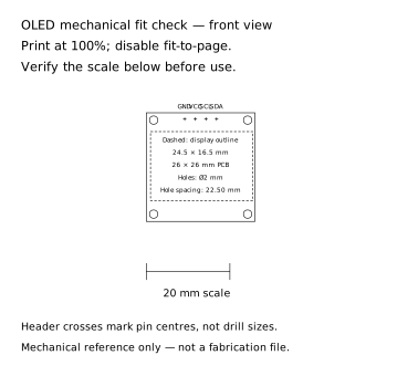


<svg xmlns="http://www.w3.org/2000/svg" width="100mm" height="90mm" viewBox="0 0 100 90">
|
||
<title>OLED module mechanical fit check — front view</title>
|
||
<desc>26 mm square PCB, four 2 mm mounting holes at 1.75 mm edge offsets. Centred four-pin header at 2.54 mm pitch, 1.50 mm from top edge. Display outline at (1, 4.5), measuring 24.5 × 16.5 mm. Header crosses indicate centres only, not drill sizes.</desc>
|
||
<g font-family="sans-serif" font-size="3" fill="black">
|
||
<text x="5" y="7">OLED mechanical fit check — front view</text>
|
||
<text x="5" y="12">Print at 100%; disable fit-to-page.</text>
|
||
<text x="5" y="17">Verify the scale below before use.</text>
|
||
</g>
|
||
<g transform="translate(35 27)" stroke="black" stroke-width="0.15" fill="none">
|
||
<rect width="26" height="26"/>
|
||
<rect id="display-outline" x="1" y="4.5" width="24.5" height="16.5" stroke-dasharray="0.6 0.4"/>
|
||
<circle cx="1.75" cy="1.75" r="1"/>
|
||
<circle cx="24.25" cy="1.75" r="1"/>
|
||
<circle cx="1.75" cy="24.25" r="1"/>
|
||
<circle cx="24.25" cy="24.25" r="1"/>
|
||
<path id="header-centres" d="M8.79 1.5h.8 M9.19 1.1v.8 M11.33 1.5h.8 M11.73 1.1v.8 M13.87 1.5h.8 M14.27 1.1v.8 M16.41 1.5h.8 M16.81 1.1v.8"/>
|
||
<g stroke="none" fill="black" font-family="sans-serif" font-size="1.5" text-anchor="middle">
|
||
<text x="9.19" y="-1">GND</text>
|
||
<text x="11.73" y="-1">VCC</text>
|
||
<text x="14.27" y="-1">SCL</text>
|
||
<text x="16.81" y="-1">SDA</text>
|
||
<text x="13" y="7">Dashed: display outline</text>
|
||
<text x="13" y="10">24.5 × 16.5 mm</text>
|
||
<text x="13" y="13">26 × 26 mm PCB</text>
|
||
<text x="13" y="16">Holes: Ø2 mm</text>
|
||
<text x="13" y="19">Hole spacing: 22.50 mm</text>
|
||
</g>
|
||
</g>
|
||
<g stroke="black" stroke-width="0.15" fill="none">
|
||
<path d="M35 65h20 M35 63v4 M55 63v4"/>
|
||
</g>
|
||
<g font-family="sans-serif" font-size="2.5" fill="black">
|
||
<text x="39" y="71">20 mm scale</text>
|
||
<text x="5" y="79">Header crosses mark pin centres, not drill sizes.</text>
|
||
<text x="5" y="84">Mechanical reference only — not a fabrication file.</text>
|
||
</g>
|
||
</svg>
|